D-type flip-flops
Categories: logic computer science

The set-reset flip-flop we looked at before was a simple type of flip-flop (or more correctly, a latch) that is easy to understand but rarely used in real applications due to its limited functionality. Here we will look at the D-type flip-flop that is commonly used in real circuits.
D-type flip-flop
A D-type flip-flop is slightly more complex than the set-reset latch, so we generally represent it as a box for simplicity:
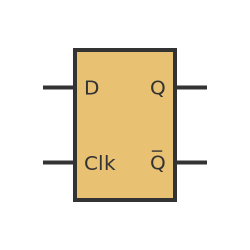
The flip-flop has 2 inputs, D (that either stands for data of delay depending on who you believe), and Clk (the clock). It has the usual 2 outputs, Q and its inverse .
Here is how it works. For most of the time the output Q retains its current value (either 1 or 0). If we change the value of the input D, that does not affect the output.
The only time the output can change is at the exact instant when Clk changes from 0 to 1. The output Q will then change to the value of D at that instant. The output is always the inverse of Q.
To be clear, it doesn't matter what happens to D at any other time, and it doesn't matter whether Clk is 0 or 1, the output never changes. Q can only change at the point when Clk goes from 0 to 1, It then stores the value of D. This means that a D-type flip-flop can be thought of as a sort of memory unit, that stores a single bit of data (0 or 1)
Flip-flop versus latch
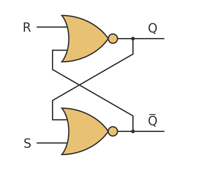
So what is the difference between a latch and a flip-flop? Here is a set-reset latch:
In a latch, the outputs change immediately in response to a change in the inputs. Here is a timeline that shows how the output Q changes as S and R change:
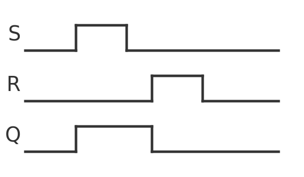
We have assumed that the gate initially has an output of 0.
When S is set to 1, this immediately sets the output to 1. When S goes back to 0, the output Q remains at 1. When R is set to 1, this immediately resets the output to 0. When R goes back to 0, the output remains at 0. A latch has the property that its output changes immediately after a relevant input change occurs.
This compares to the timeline for a D-type flip-flop:
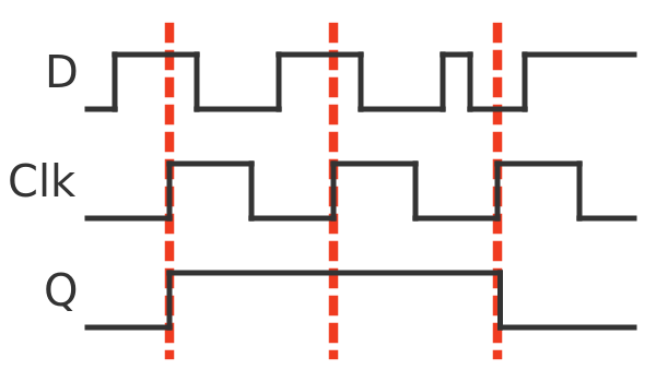
In this example, the data input D changes quite frequently. But, as we saw earlier, the value of Q only changes at the exact point where the Clk switches from 0 to 1. Each of these time points is marked with a dashed red line.
On the first clock edge, Q is set to 1 because D is 1. On the second clock it remains at 1 because D is still 1.On the third clock it goes back to 0 because D is 0.
If D changes at any other time, no matter whether Clk is 0 or 1, the output is not affected. Using clocked flip-flops helps to solve a serious problem with complex logic circuits (such as CPUs) as we will see next.
Using D-type flip-flops to avoid timing problems
To see the advantage of a clocked flip-flop, consider this simple logic circuit that uses an adder:
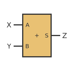
This circuit has 2 inputs, X and Y. It calculates the binary sum of the 2 input bits and outputs the result as Z.
An important thing to remember about this circuit is that it takes a finite amount of time to calculate the result. If we change the values of X and Y, the value of Z doesn't change instantly, it takes a short time for the output to respond to the change in input values. This time is very small (it can be in the range of picoseconds for a high-speed CPU) but it cannot be ignored.
We need to design our circuit to ensure that Z is not used until it is ready.
In a real adder circuit, perhaps where 64-bit numbers are being added, the circuit would use 64 separate adder blocks, and the carry bit would have to be propagated from one adder to the next. There are ways to mitigate this problem but even then it can take longer for a multi-bit adder to stabilise than it does for a 1-bit adder.
Again we need to make sure the outputs of the adder are not used until they are ready, but this is now slightly more complicated because there are more gates and signals involved.
In a more complex circuit the output Z would be fed into another logic block, maybe to get shifted or multiplied, and the output of that next stage would be delayed again. In a highly complex circuit like a CPU, with many millions of gates, every signal at every point might become valid at a different time and the overall circuit design would have to somehow take account of all the delays. That really wouldn't be practical for a complex circuit.
Clock synchronisation
A solution to this problem is to use a clock signal to synchronize everything. We can do this by using flip-flops to store intermediate results. For example:
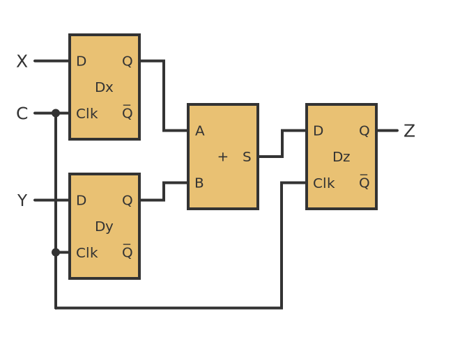
The structure of the circuit has 3 layers:
- D-type flip-flops Dx and Dy that are used to store the input values.
- An adder circuit, just like the previous simple example.
- D-type flip-flop Dz that stores the output value.
All the D-type flip-flops are controlled by the same clock signal, C. This clock signal is continuously alternating between 0 and 1. This signal alternates at several GHz - that is, billions of times per second - in a modern CPU.
Now let's look at the operation in more detail. The following sequence of events occurs:
- Inputs X and Y are set to the required values.
- When the clock signal goes from 0 to 1, the values of X and Y are transferred to the Q outputs of Dx and Dy.
- The adder adds the 2 inputs to create a result S.
- When the clock signal goes from 0 to 1 again, the value of S is transferred to the Z (which is the Q output of Dz).
- So when we set X and Y, we can guarantee that, 2 clock cycles later, Z will be correct.
This, of course, assumes that the clock runs at a rate that allows the outputs of each step to stabilise before the next tick of the clock. The faster the gates in the circuit operate, the faster we can clock the chip. The CPUs used in the first popular home computers (such as the ZX Spectrum) in the early 80s were clocked at a few Mhz. At the time of writing most PCs are clocked at several GHz, about 1000 times faster.
Paralleling and pipelining
The system described above means that many operations will take multiple clock cycles to perform. This may seem wasteful, but we have seen that it is worthwhile (in fact necessary) to avoid very significant design problems. However, there are ways to improve the overall speed of a complex circuit even given that limitation. We can attempt to do more than one thing at once.
The simplest way to do this is parallelisation. In the example above our circuit can only process a certain number of data bits per second. But if we had 2 separate adder circuits, we could process twice as many bits per second. With more circuits, the performance could be increased even more.
Most modern CPUs have multiple cores. A core contains everything necessary to run a program on its own, so if a CPU has 4 cores then loosely speaking it can run 4 programs concurrently. More precisely, it can run 4 threads. Each thread might be a separate program, but in some cases, the same program can run on multiple cores if it has been written to support multi-threading.
In addition, some of the circuitry within the core might be duplicated. For instance, it is common for a core to include more than one ALU, so that several arithmetic calculations can be done at the same time. This is usually controlled by the core itself and doesn't require the software to be written in any special way.
A second way to speed up processing is via pipelining. In the example above, it takes 2 clock cycles for the data to be read, added, and made available on the output. But that doesn't mean we can only add 1 set of values every 2 clock cycles. Imagine we have several sets of data to process: (X1, Y1), (X2, Y2), (X3, Y3)... We could do this:
- First clock read X1 and Y1 into Dx and Dy.
- Second clock transfer the sum S1 into Dz so it is available as Z. At the same time read X2 and Y2 into Dx and Dy.
- Third clock transfer the sum S2 into Dz so it is available as Z. At the same time read X3 and Y3 into Dx and Dy.
- And so on...
This doubles throughput without any significant extra hardware.
D-type flip-flop implementation - D-type latch
A D-type flip-flop can be created from an SR latch, by adding extra logic to control its inputs. First, we will look at a slightly simpler case, the D-type latch:
If you are familiar with a set-reset latch, you might notice that the 2 gates X and Y form a NOR gate SR-latch, with inputs R and S. This has the following rules:
- If R is 1 and S is 0, output Q is set to 0.
- If R is 0 and S is 1, output Q is set to 1.
- If R is 0 and S is 0, output Q is will remain in whatever its previous state was.
- R is 1 and S is 1 is a disallowed state.
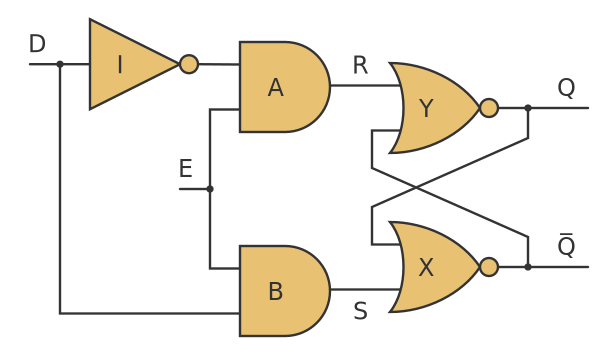
In the D-type latch, we add some extra gates, the 2 AND gates A and B plus a NOT gate I. We will consider the 2 cases when E is 1 or 0.
When E is 1, the 2 AND gates depend only on the input D:
- When D is 0, the input to gate A will be 1, so the R input of the SR-latch will be 1. This will reset Q to 0.
- When D is 1, the input to gate B will be 1, so the S input of the SR-latch will be 1. This will set Q to 1.
In other words, when E is 1, the output Q will follow D. The name E stands for enable.
When E is 0, the 2 AND gates will both have outputs of 0. This means that S and R will both be 0, so Q will be latched at whatever its previous value was.
So when E is 1 Q will follow D, but when E goes to 0 then Q will stick remember the latest value of D. This is kind of like a D-type flip-flop, but we call it a latch because its output sometimes follows the input.
D-type flip-flop
There are various ways that we can transform a D-type latch into a flip-flop. The simplest, slightly hacky, way is to add this little circuit before the enable input E:
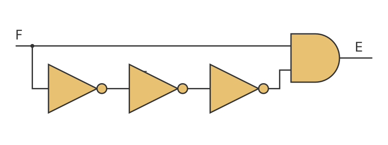
What does this circuit do? Well first, consider the 3 NOT gates in a row. Inverting a signal 3 times (not, not, not) is logically equivalent to inverting it once. So in purely logical terms (assuming infinitely fast gates), we have an AND gate that is fed by 2 signals - F and the inverse of F. Since one or the other of those signals has to be 0, the output is always 0. Here is a timeline:
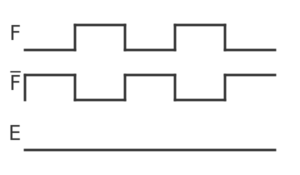
There is never a time when both inputs are 1, so the output of the AND gate is always 0.
But real gates are not infinitely fast. If we change the input of a gate, it takes a finite amount of time for the output to respond. And in our circuit, we have 3 NOT gates in a row, so that takes 3 times as long as the normal gate response time.
The signal F goes directly to the AND gate, but the inverse signal is delayed, so the timeline looks like this:
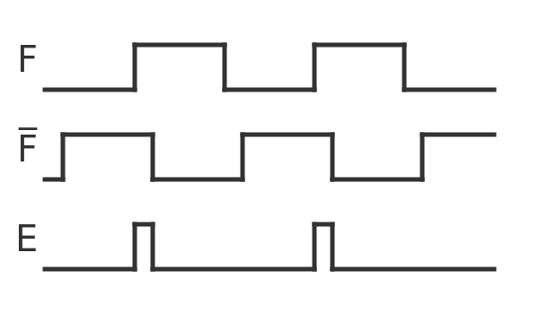
Each time F goes positive, there is a brief period when both inputs are 1, which creates a short pulse on E. The reason we use 3 NOT gates rather than just 1 is to make the pulse slightly longer. If the pulse is too short there is a possibility that the flip-flop might not respond.
By feeding this modified signal into the E input of a D-type latch, we simulate a D-type flip-flop. This is still technically a latch, because while E is at 1 to output Q will still follow the input D. But if the overall circuit is properly designed, D should be stable at the point when the clock occurs, so this should not be a problem.
There are several other ways to design a D-type flip-flop, but we won't cover them here.
Related articles
Join the GraphicMaths Newsletter
Sign up using this form to receive an email when new content is added to the graphpicmaths or pythoninformer websites:
Popular tags
adder adjacency matrix alu and gate angle answers area argand diagram binary maths cardioid cartesian equation chain rule chord circle cofactor combinations complex modulus complex numbers complex polygon complex power complex root cosh cosine cosine rule countable cpu cube decagon demorgans law derivative determinant diagonal differential equation directrix dodecagon e eigenvalue eigenvector einstein ellipse equilateral triangle erf function euclid euler eulers formula eulers identity exercises exponent exponential exterior angle first principles flip-flop focus gabriels horn galileo gamma function gaussian distribution gradient graph hendecagon heptagon heron hexagon hilbert horizontal hyperbola hyperbolic function hyperbolic functions infinity integration integration by parts integration by substitution interior angle inverse function inverse hyperbolic function inverse matrix irrational irrational number irregular polygon isomorphic graph isosceles trapezium isosceles triangle kite koch curve l system lhopitals rule limit line integral locus logarithm maclaurin series major axis matrix matrix algebra mean minor axis n choose r nand gate net newton raphson method nonagon nor gate normal normal distribution not gate octagon or gate parabola parallelogram parametric equation pentagon perimeter permutation matrix permutations pi pi function polar coordinates polynomial power probability probability distribution product rule proof pythagoras proof pythagorean triple quadrilateral questions quotient rule radians radius rectangle regular polygon rhombus root sech segment set set-reset flip-flop simpsons rule sine sine rule sinh slope sloping lines solving equations solving triangles special relativity speed of light square square root squeeze theorem standard curves standard deviation star polygon statistics straight line graphs surface of revolution symmetry tangent tanh transformation transformations translation trapezium triangle turtle graphics uncountable variance vertical volume volume of revolution xnor gate xor gate